Metalens Technology: Transforming Consumer Electronics Today
Metalens technology represents a significant leap forward in the field of optics, merging innovation with practicality to revolutionize how we manipulate light. Developed in the Harvard lab of Federico Capasso, these mini-lens devices utilize advanced metasurfaces that enable mass production of lightweight lenses, paving the way for their integration in a multitude of consumer electronics. Rob Devlin, CEO of the startup Metalenz, has played a crucial role in transforming this optical innovation from lab experiments to real-world applications, producing millions of units for gadgets such as smartphones and tablets. By leveraging semiconductor chip foundries, metalenses drastically reduce the size and cost of conventional lenses while enhancing optical performance. As more industries recognize the potential of mini-lens technology, the future of photography and 3D sensing looks brighter with the promise of unprecedented advancements.
The emergence of lens technology that employs metasurfaces marks a new era of optical engineering, bringing forth alternatives to traditional lens systems. These groundbreaking devices, often referred to as mini-lenses, stand out for their ability to significantly reduce size and weight while maintaining, or even enhancing, optical functions. Spearheaded by visionaries like Rob Devlin and his team at Metalenz, this approach allows for the creation and mass production of advanced optical components, facilitating their use in everyday devices. With roots in university startups like Metalenz and the pioneering work of researchers at Harvard, this optical innovation is transforming industries by enabling compact designs suitable for modern technology demands. As developments in this field progress, the integration of metasurfaces in consumer electronics continues to reshape the landscape of optical solutions.
Understanding Metalens Technology and Its Impact
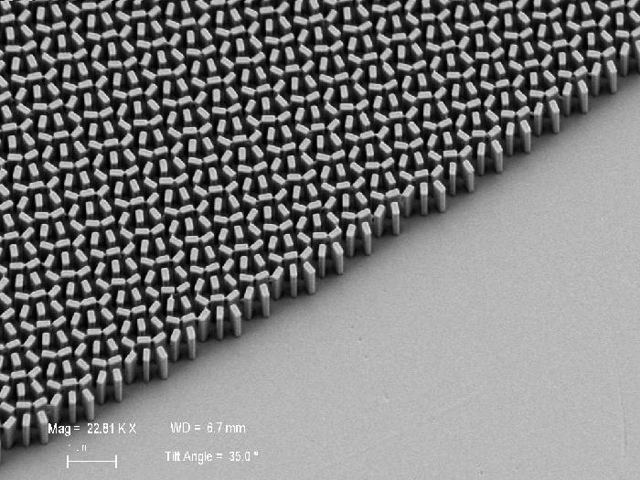
Metalens technology represents a significant leap in optical innovation, providing a compact and efficient solution for light manipulation. Unlike traditional lenses, which require glass or plastic molds, metalenses utilize nanostructured metasurfaces made of tiny pillars. This futuristic approach allows for miniaturization without sacrificing functionality, paving the way for their integration into consumer electronics. The shift from conventional lenses to metalenses not only reduces bulk but also enhances the performance of devices such as smartphones and tablets by allowing more sophisticated features without added weight.
The transition of metalens technology from concept to commercial application showcases the potential of university startups like Metalenz. Rob Devlin, instrumental in this evolution, transformed academic research into a viable product that is now breathing new life into the optics industry. As demand for smaller and more efficient components in consumer devices surges, the capability of metasurfaces to focus light with unprecedented precision holds promise for future advancements in technology beyond mere portability.
From University Labs to Consumer Electronics
The journey of metalens technology from the Capasso lab at Harvard to the consumer market exemplifies how university research can disrupt traditional industries. Rob Devlin was pivotal in this transformation, leveraging knowledge gained during his doctoral studies to innovate mini-lenses that could outshine traditional optical components. With a blend of scientific expertise and entrepreneurial spirit, university startups like Metalenz can harness groundbreaking research to deliver cutting-edge products that meet real-world needs.
The rapid adaptation of the lenses from lab prototypes to mass-produced components is a testament to the effectiveness of collaboration across academic disciplines. As highlighted by industry leaders like Sam Liss, it’s this fusion of scientific backgrounds and innovative thinking that drives real progress. By embracing a mindset of disruption and exploration, Metalenz reflects the spirit of contemporary university research, creating not just products but entirely new industries that reshape our interaction with technology.
The Evolution of Optical Innovations
Optical innovations such as metalenses are redefining how we perceive and interact with technology in our daily lives. These advancements stem from rigorous research, with milestones like the publication of seminal papers detailing the capabilities of metasurfaces. The capabilities demonstrated by researchers, notably in the Capasso lab, set the stage for a new trajectory in optics that goes beyond conventional wisdom. Such innovations promise to enable devices that can perform multiple functions in a fraction of the space.
Moreover, the development of metalens technology challenges engineers and designers to rethink existing paradigms in product design. As traditional optics continue to face limitations in miniaturization and integration, metasurfaces offer a viable alternative that could catalyze the next wave of consumer electronics. The future will likely see even more revolutionary applications arising from the ongoing refinement of optical technologies, echoing sentiments from industry experts that we have only scratched the surface of what’s possible.
Challenges and Opportunities in Optical Technology
As the startup Metalenz rises to prominence, it also faces challenges inherent to the rapidly evolving field of optical technologies. Manufacturing at scale involves navigating complex supply chains and ensuring the quality of each metasurface produced. Companies must balance the urgency of market demand with the necessity of maintaining high standards to avoid compromising performance. Innovations in semi-conducting manufacturing, however, are reshaping these hurdles, providing new avenues for rapid production of metalenses.
At the same time, the optical innovation sector is brimming with opportunity. As Rob Devlin and his team push forward with plans for future product lines like Polar ID, the versatility of metasurfaces can catalyze groundbreaking applications in various industries—including health technology, augmented reality, and environmental monitoring. This dynamic interplay of challenges and opportunities exemplifies the nature of scientific advancement, where each hurdle can lead to innovation that further shapes the future of technology.
The Role of Collaboration in Advancing Technology
The successful evolution of metalens technology underscores the importance of collaboration within academia and industry. Partnerships between researchers and entrepreneurs, as witnessed at Metalenz, are pivotal in transforming theoretical science into practical applications. By fostering an environment where academic insight meets market needs, stakeholders can co-create products that not only demonstrate scientific prowess but also appeal to consumers looking for better, smarter devices.
Additionally, collaborative ventures allow for the diverse exchange of ideas, critical for pushing the boundaries of optical science. As prominent partnerships continue to form, there’s an opportunity for ongoing discovery and enhancement of metasurfaces that could eventually revolutionize other domains within technology. The future looks promising, provided the spirit of collaboration persists, driving innovations that harness the true potential of optical advancements.
Future Prospects of Polarization in Technology
The integration of polarization technologies, such as Metalenz’s Polar ID, signals a new frontier in the capabilities of consumer electronics. By measuring the unique polarization signatures that objects emit, devices can gain a significant edge in security and feature integration. Such advancements can enhance user experiences while providing a layer of protection that traditional sensors lack. The emergence of this polarization metasurface promises to make sophisticated imaging and sensing technologies more accessible and cost-effective.
With the possibilities of detecting skin cancer and monitoring air quality being just a couple of examples, the potential applications of polarization in technology are vast. As industry players like Metalenz continue to innovate, we can expect to see broader implementations of this technology across various sectors, including healthcare and environmental sciences. This evolution reinforces the transformative impact of optical innovation in real-world applications, illustrating how advanced technologies can lead to improved safety and efficiency.
The Economic Impact of Metalens Technology
As Metalenz scales production of its metalenses, the associated economic impact becomes increasingly evident. By sourcing manufacturing processes from established semiconductor foundries, the startup not only helps to lower production costs but also fuels job creation within the tech industry. The ripple effect of such innovations can lead to a more competitive market, benefiting consumers through better pricing and performance of electronic devices equipped with metalenses.
In the broader context, the proliferation of such optical technologies could stimulate growth in various sectors. From smartphones that become lighter and more efficient to smart devices that harness 3D sensing for augmented reality, the return on investment for developed technologies like Metalenz isn’t just about improved products but also about fostering whole new industries. As this technology proliferates, it sets the stage for potentially transformative economic advancements.
The Environmental Considerations of Metalens Production
In an era where sustainability is paramount, the environmental implications of metalens production warrant attention. By utilizing semiconductor manufacturing processes that prioritize efficiency and precision, companies like Metalenz can minimize waste compared to traditional glass and plastic lens production. Emphasizing eco-friendly practices within manufacturing not only benefits the planet but also aligns with the increasing consumer demand for environmentally considerate products.
Moreover, the compact size of metalenses enables the production of smaller devices that require fewer resources throughout their lifecycle. As innovations in optical technologies continue to evolve, a focus on sustainable production methods and responsible consumption will be crucial in shaping how future electronic devices are developed. This commitment to sustainability may provide a competitive advantage in a market increasingly driven by eco-conscious consumers.
Metalens Technology and Its Global Implications
The implications of metalens technology extend far beyond individual consumer electronics; they have the potential to influence global markets. As manufacturers worldwide adopt this advanced optical innovation, we could witness shifts in the competitive landscape of tech companies. Nations prioritizing semiconductor manufacturing capabilities will likely gain leverage in this rapidly evolving sector, creating new dynamics in international trade and innovation.
Furthermore, as metalens technology becomes more prevalent, it may drive advancements in fields like telecommunications and autonomous vehicles, where compact and efficient optical systems are crucial. This technological proliferation indicates a future where countries investing in optical innovations and university research may emerge as leaders in the global economy. The adaptability and functionality of metalenses hold the promise to usher in a new era of technological growth on a worldwide scale.
Frequently Asked Questions
What is metalens technology and how does it differ from traditional lenses?
Metalens technology utilizes metasurfaces made up of tiny pillars to manipulate light, allowing it to function like traditional lenses but in a much smaller and thinner format. Unlike conventional lenses that require curved glass or plastic, metalenses can be produced on millimeter-thin wafers, making them cheaper and easier to mass produce. This innovation in optics is a significant advancement in optical engineering.
How are mini-lenses produced using metalens technology impacting consumer electronics?
The production of mini-lenses through metalens technology is revolutionizing consumer electronics by enabling slimmer designs without compromising on functionality. These metasurfaces are currently integrated into devices like smartphones and tablets, allowing for advanced features such as facial recognition and 3D sensing, thanks to the efficient light-manipulating properties of the mini-lenses.
Who is Rob Devlin and what role did he play in the development of metalens technology?
Rob Devlin is the CEO of Metalenz, a startup that commercializes metalens technology. During his Ph.D. at Harvard, he significantly contributed to the creation of metalenses by experimenting with materials and designs, leading to the development and mass production of highly efficient metasurfaces that are now used in various consumer devices.
What are the advantages of using metasurfaces in optical innovation?
The advantages of using metasurfaces in optical innovation include their ability to manipulate light more effectively than traditional optics, potentially reducing the size and cost of optical modules. This technology can simplify complex optical systems and provide enhanced functionalities, paving the way for new applications in smart devices, augmented reality, and advanced sensing technologies.
How does Metalenz plan to expand its applications of metalens technology in the future?
Metalenz aims to expand the applications of its metalens technology by continuing to enhance the performance of existing products and exploring new functionalities, such as Polar ID, which utilizes light polarization for improved security measures. The focus is on creating cost-effective solutions that can be widely adopted in various devices, thus leveraging the unique properties of metasurfaces.
What role did university startups play in the advancement of metalens technology?
University startups like Metalenz play a crucial role in advancing metalens technology by transitioning groundbreaking research from academic labs into commercial products. This process not only commercializes innovative technologies developed in university settings but also disrupts traditional industries by introducing more efficient and cost-effective optical solutions.
| Key Aspect | Details |
|---|---|
| Founder | Rob Devlin, former graduate student at Harvard. |
| Technology Origin | Developed in Federico Capasso’s lab, focusing on light manipulation using mini-lenses. |
| Mass Production | Metalenz has produced about 100 million metasurfaces for consumer devices. |
| Applications | Used in iPads, Samsung Galaxy S23 Ultra, and Google Pixel 8 Pro, primarily for 3D sensing. |
| Future Developments | Working on Polar ID, a new security feature for smartphones using polarization. |
| Market Impact | Metalenz’s technology is disrupting traditional lens manufacturing to enhance device compactness. |
Summary
Metalens technology is revolutionizing the optics industry by enabling light manipulation through innovative mini-lenses that are smaller, cheaper, and more efficient than traditional lenses. This groundbreaking advancement originated from research at Harvard University and has evolved into practical applications in consumer electronics. With millions of units manufactured and deployed, Metalenz is setting the stage for continued disruption in optical technology, paving the way for future innovations like the Polar ID system.